- 您现在的位置:买卖IC网 > Sheet目录251 > SFCF64GBH2BU4TO-I-NU-517-STD (Swissbit NA Inc)FLASH SLC UDMA/MDMA/PIO 64GB
�� �
�
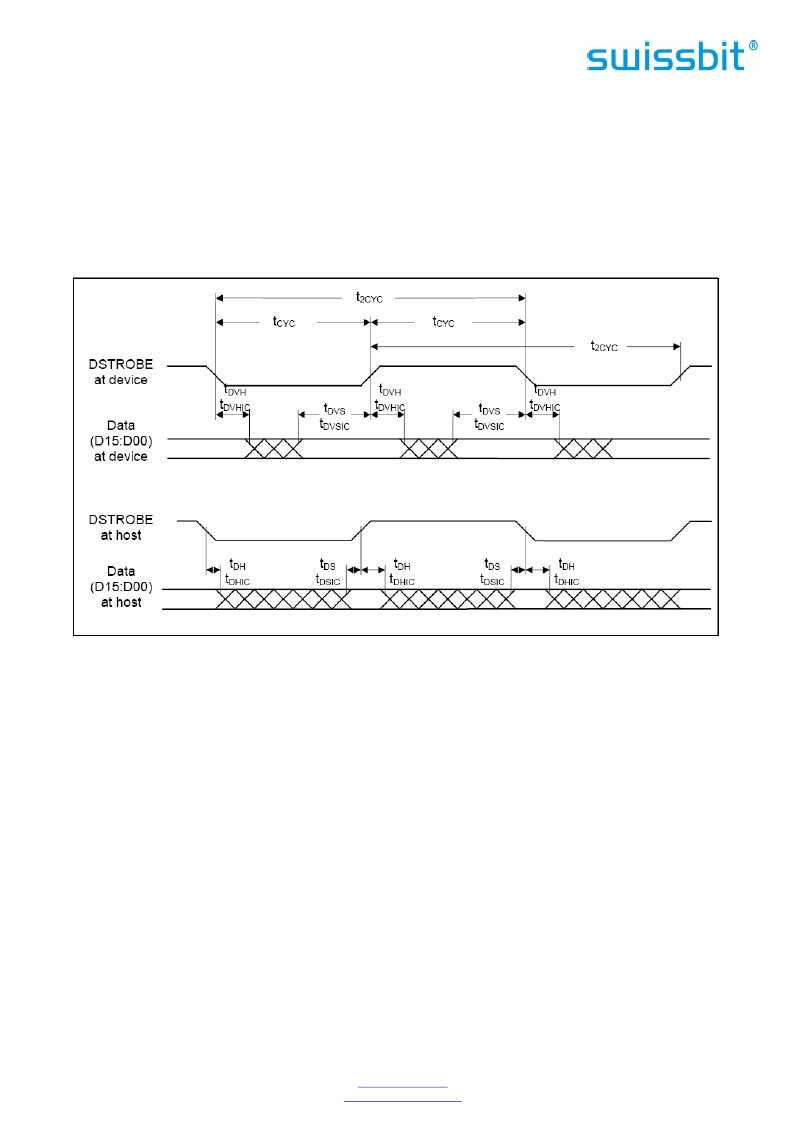
�The� following� steps� shall� occur� in� the� order� they� are� listed� unless� otherwise� specifically� allowed:�
�a)� The� device� shall� drive� a� data� word� onto� D[15:0].�
�b)� The� device� shall� generate� a� DSTROBE� edge� to� latch� the� new� word� no� sooner� than� t� DVS� after� changing� the�
�state� of� D[15:0].� The� device� shall� generate� a� DSTROBE� edge� no� more� frequently� than� t� CYC� for� the� selected�
�Ultra� DMA� mode.� The� device� shall� not� generate� two� rising� or� two� falling� DSTROBE� edges� more� frequently�
�than� 2tcyc� for� the� selected� Ultra� DMA� mode.�
�c)�
�The� device� shall� not� change� the� state� of� D[15:0]� until� at� least� tDVH� after� generating� a� DSTROBE� edge� to�
�latch� the� data.�
�d)� The� device� shall� repeat� steps� (a),� (b),� and� (c)� until� the� data� transfer� is� complete� or� an� Ultra� DMA� burst� is�
�paused,� whichever� occurs� first.�
�Figure� 11:� Sustained� Ultra� DMA� Data-In� Burst� Timing�
�Notes:� D[15:0]� and� DSTROBE� signals� are� shown� at� both� the� host� and� the� device� to� emphasize� that� cable� settling�
�time� as� well� as� cable� propagation� delay� shall� not� allow� the� data� signals� to�
�be� considered� stable� at� the� host� until� some� time� after� they� are� driven� by� the� device.�
�6.5.4.4.3� Host� Pausing� an� Ultra� DMA� Data-In� Burst�
�The� host� pauses� a� Data-In� burst� by� following� the� steps� lettered� below.� A� timing� diagram� is� shown� in� Figure� 12:�
�Ultra� DMA� Data-In� Burst� Host� Pause� Timing.� The� timing� parameters� are� specified� in� Table� 26:� Ultra� DMA� Data� Burst�
�Timing� Requirements� and� are� described� in� Table� 27:� Ultra� DMA� Data� Burst� Timing� Descriptions.�
�The� following� steps� shall� occur� in� the� order� they� are� listed� unless� otherwise� specifically� allowed:�
�a)� The� host� shall� not� pause� an� Ultra� DMA� burst� until� at� least� one� data� word� of� an� Ultra� DMA� burst� has� been�
�transferred.�
�b)� The� host� shall� pause� an� Ultra� DMA� burst� by� negating� –� HDMARDY.�
�c)� The� device� shall� stop� generating� DSTROBE� edges� within� t� RFS� of� the� host� negating� –� HDMARDY.�
�d)� If� the� host� negates� –� HDMARDY� within� t� SR� after� the� device� has� generated� a� DSTROBE� edge,� then� the� host�
�shall� be� prepared� to� receive� zero� or� one� additional� data� words.� If� the� host� negates� –� HDMARDY� greater�
�than� t� SR� after� the� device� has� generated� a� DSTROBE� edge,� then� the� host� shall� be� prepared� to� receive� zero,�
�one� or� two� additional� data� words.� The� additional� data� words� are� a� result� of� cable� round� trip� delay� and� t� RFS�
�timing� for� the� device.�
�e)� The� host� shall� resume� an� Ultra� DMA� burst� by� asserting� –� HDMARDY.�
�Swissbit� AG�
�Industriestrasse� 4�
�Swissbit� reserves� the� right� to� change� products� or� specifications� without� notice.�
�Revision:� 1.00�
�CH-9552� Bronschhofen�
�Switzerland�
�www.swissbit.com�
�industrial@swissbit.com�
�C-440_data_sheet_CF-HxBU_Rev100.doc�
�Page� 32� of� 102�
�发布紧急采购,3分钟左右您将得到回复。
相关PDF资料
SFN08B4702CBQLF7
RES ARRAY 47K OHM 7 RES 8-DFN
SFP1050-12BG
FRONT END AC/DC 1050W 12V
SFP450-12BG
PWR SUP 450W 12V 36.6A W/STANDBY
SFSD1024N1BN1TO-I-DF-151-STD
FLASH MICRO SD CARD IND S-200 1G
SFSD2048L1BN2TO-I-DF-151-STD
FLASH SECURE DGTL CARD SD 2G
SFSD4096L1BN2TO-I-Q2-141-STD
FLASH SECURE DGTL CARD SDHC 4G
SFSD8192N1BW1MT-E-QG-111-STD
FLASH MICRO SD 8GB EXT TEMP
SFUI4096J1BP2TO-I-DT-211-STD
FLASH DRIVE USB MODULE U-110 4G
相关代理商/技术参数
SFCF64GBH2BU4TO-I-NU-527-STD
制造商:SWISSBIT 功能描述:CFC C-440 DENSITY INDUSTRIAL - Trays 制造商:SWISSBIT NA INC 功能描述:FLASH CARD 64GB IND C-440 制造商:Swissbit 功能描述:Memory Cards 64GB IND COMPACT FLASH SLC NAND C440
SFCF8192H1BO2TO-C-Q1-523-SMA
制造商:SWISSBIT NA INC 功能描述:FLASH
SFCF8192H1BO2TO-C-Q1-533-ZP1
制造商:SWISSBIT NA INC 功能描述:FLASH
SFCF8192H1BO2TO-C-Q1-543-SMA
制造商:SWISSBIT NA INC 功能描述:FLASH
SFCF8192H1BO2TOIQ1523SMA
制造商:Swissbit 功能描述:Flash Card 8G-Byte 3.3V/5V CompactFlash 50-Pin
SFCF8192H1BO2TO-I-Q1-523-SMA
功能描述:FLASH SLC UDMA/MDMA/PIO 8G RoHS:是 类别:存储卡,模块 >> 存储器,PC 卡 系列:C-320 标准包装:30 系列:- 存储容量:8GB 存储器类型:存储卡 - Extreme III SD?
SFCF8192H1BO2TO-I-Q1-533-ZP1
制造商:SWISSBIT NA INC 功能描述:FLASH
SFCF8192H1BO2TO-I-Q1-543-SMA
制造商:SWISSBIT NA INC 功能描述:FLASH